Technical Documents
Specifications
Brand
MicrochipMemory Size
256kB
Product Type
EEPROM
Interface Type
Serial-SPI
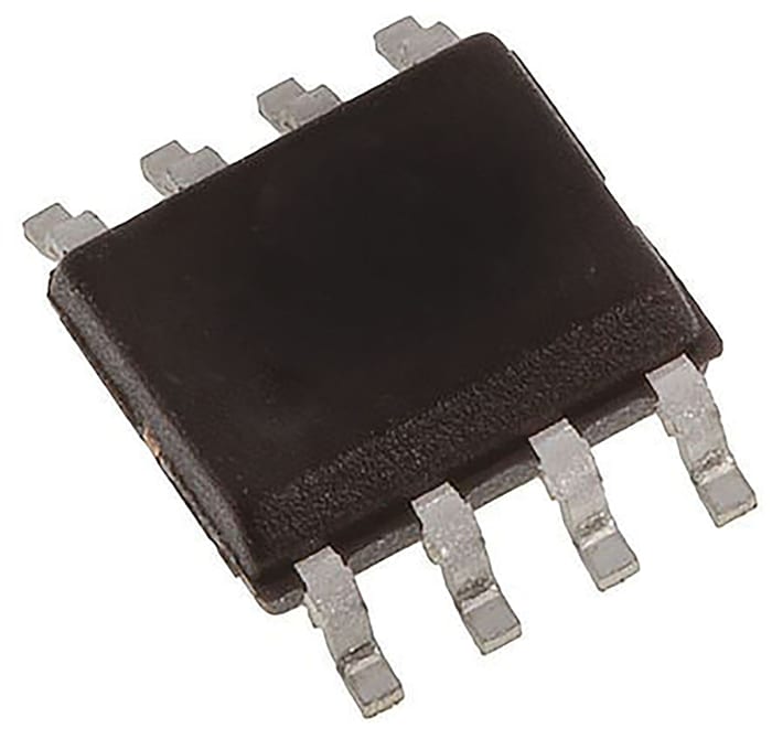
Package Type
SOIC
Mount Type
Surface
Pin Count
8
Maximum Clock Frequency
10MHz
Organisation
256 kB
Minimum Supply Voltage
2.5V
Number of Bits per Word
8
Maximum Supply Voltage
5.5V
Minimum Operating Temperature
-40°C
Maximum Operating Temperature
125°C
Height
1.75mm
Length
4.9mm
Standards/Approvals
No
Width
1.75mm
Series
25LC256
Data Retention
200year
Supply Current
6mA
Maximum Random Access Time
50ns
Automotive Standard
AEC-Q100
Number of Words
32768
Product Details
Microchips 25AA256/25LC256 family of devices are 256 Kbit SPI Serial EEPROMs available in a variety of package, temperature and power supply variants.
The Serial Peripheral Interface (SPI) is utilised to provide the required Clock Input (SCK), Data In (SI) and Data Out (SO) signals. The operation of these devices can be paused via a Hold pin (HOLD) which causes inputs to be ignored with the exception higher priority interrupts defined via the Chip Select (CS) pin.
Stock information temporarily unavailable.
P.O.A.
Each (Supplied in a Tube) (ex VAT)
Production pack (Tube)
5
P.O.A.
Each (Supplied in a Tube) (ex VAT)
Stock information temporarily unavailable.
Production pack (Tube)
5
Technical Documents
Specifications
Brand
MicrochipMemory Size
256kB
Product Type
EEPROM
Interface Type
Serial-SPI
Package Type
SOIC
Mount Type
Surface
Pin Count
8
Maximum Clock Frequency
10MHz
Organisation
256 kB
Minimum Supply Voltage
2.5V
Number of Bits per Word
8
Maximum Supply Voltage
5.5V
Minimum Operating Temperature
-40°C
Maximum Operating Temperature
125°C
Height
1.75mm
Length
4.9mm
Standards/Approvals
No
Width
1.75mm
Series
25LC256
Data Retention
200year
Supply Current
6mA
Maximum Random Access Time
50ns
Automotive Standard
AEC-Q100
Number of Words
32768
Product Details
Microchips 25AA256/25LC256 family of devices are 256 Kbit SPI Serial EEPROMs available in a variety of package, temperature and power supply variants.
The Serial Peripheral Interface (SPI) is utilised to provide the required Clock Input (SCK), Data In (SI) and Data Out (SO) signals. The operation of these devices can be paused via a Hold pin (HOLD) which causes inputs to be ignored with the exception higher priority interrupts defined via the Chip Select (CS) pin.