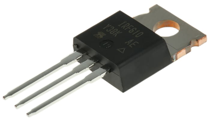
N-Channel MOSFET Transistor, 3.3 A, 200 V, 3-Pin TO-220AB Fairchild IRF610

Technical documents
Specifications
Channel Type
N
Maximum Continuous Drain Current
3.3 A
Maximum Drain Source Voltage
200 V
Package Type
TO-220AB
Mounting Type
Through Hole
Pin Count
3
Maximum Drain Source Resistance
1.5 Ω
Channel Mode
Enhancement
Maximum Power Dissipation
43 W
Maximum Gate Source Voltage
-20 V, +20 V
Width
4.83mm
Typical Gate Charge @ Vgs
5.3 nC @ 10 V
Number of Elements per Chip
1
Maximum Operating Temperature
+150 °C
Length
10.67mm
Minimum Operating Temperature
-55 °C
Height
9.4mm
Product details
Enhancement Mode N-Channel MOSFET, Fairchild Semiconductor
Enhancement Mode Field Effect Transistors (FET) are produced using Fairchild’s proprietary, high cell density, DMOS technology. This high density process has been designed to minimise on-state resistance, provide rugged and reliable performance and fast switching.
MOSFET Transistors, ON Semi
ON Semi offers a substantial portfolio of MOSFET devices that includes high-voltage (>250V) and low-voltage (<250V) types. The advanced silicon technology provides smaller die sizes, which it is incorporated into multiple industry-standard and thermally-enhanced packages.
ON Semi MOSFETs provide superior design reliability from reduced voltage spikes and overshoot, to lower junction capacitance and reverse recovery charge, to elimination of additional external components to keep systems up and running longer.
P.O.A.
Standard
1
P.O.A.
Stock information temporarily unavailable.
Standard
1
Stock information temporarily unavailable.
| quantity | Unit price |
|---|---|
| 1 - 24 | P.O.A. |
| 25 - 99 | P.O.A. |
| 100 - 249 | P.O.A. |
| 250 - 499 | P.O.A. |
| 500+ | P.O.A. |
Technical documents
Specifications
Channel Type
N
Maximum Continuous Drain Current
3.3 A
Maximum Drain Source Voltage
200 V
Package Type
TO-220AB
Mounting Type
Through Hole
Pin Count
3
Maximum Drain Source Resistance
1.5 Ω
Channel Mode
Enhancement
Maximum Power Dissipation
43 W
Maximum Gate Source Voltage
-20 V, +20 V
Width
4.83mm
Typical Gate Charge @ Vgs
5.3 nC @ 10 V
Number of Elements per Chip
1
Maximum Operating Temperature
+150 °C
Length
10.67mm
Minimum Operating Temperature
-55 °C
Height
9.4mm
Product details
Enhancement Mode N-Channel MOSFET, Fairchild Semiconductor
Enhancement Mode Field Effect Transistors (FET) are produced using Fairchild’s proprietary, high cell density, DMOS technology. This high density process has been designed to minimise on-state resistance, provide rugged and reliable performance and fast switching.
MOSFET Transistors, ON Semi
ON Semi offers a substantial portfolio of MOSFET devices that includes high-voltage (>250V) and low-voltage (<250V) types. The advanced silicon technology provides smaller die sizes, which it is incorporated into multiple industry-standard and thermally-enhanced packages.
ON Semi MOSFETs provide superior design reliability from reduced voltage spikes and overshoot, to lower junction capacitance and reverse recovery charge, to elimination of additional external components to keep systems up and running longer.